


Views: 0 Author: Site Editor Publish Time: 2026-09-04 Origin: Site


As module wattages increase rapidly, manufacturing wafers become increasingly thinner. This dangerous combination accelerates production-line yield losses. Invisible defects cause these costly drops. Today, standard visual quality control is no longer sufficient. Traditional checks fail completely when assessing larger, thinner formats like 182mm and 210mm wafers. These massive physical dimensions magnify material fragility exponentially.
When undetected solar cell microcracks escape the factory floor, they ruin final module performance. These hidden faults also expose manufacturers to severe liability claims from frustrated end-users. This article gives production managers and procurement directors a definitive evaluation framework. We will help you evaluate essential process upgrades effectively. You will discover practical equipment strategies designed to minimize mechanical and thermal stress. We also explore integrating advanced inspection technologies seamlessly into your gigawatt-scale lines. Ultimately, mastering these proactive strategies protects your Tier-1 manufacturing credibility and safeguards long-term product reliability.
Upgrading to larger wafers (M10 and G12) requires recalibrating robotic handling and thermal profiles to prevent catastrophic yield drops.
In-line Electroluminescence (EL) testing integrated with AI is the only verifiable method for identifying microcracks before lamination.
Preventative equipment upgrades must be evaluated on a matrix of throughput speed, tension control, and thermal uniformity to ensure ROI.
Mitigating solar cell microcracks directly reduces warranty liabilities and protects Tier-1 manufacturing credibility.
A single microcrack escaping your facility creates compounding financial failures. These tiny fissures expand during shipping and field installation. This expansion leads directly to module degradation and severe hot spots. Customers then file massive warranty claims. Consequently, your brand suffers heavy reputational damage. We must stop these defects at the source.
The industry shift toward larger, high-efficiency cells makes things worse. Fragility increases alongside physical dimensions. A G12 TOPCon Solar Cell measures 210mm across. It faces exponentially higher mechanical bending stress during factory transit. Older, smaller formats rarely experienced such severe deflection. Manufacturers must rethink their handling limits entirely to accommodate these wider spans.
Thermal stress also varies wildly between cell technologies. The unique thermal processing requirements of an M10 TOPCon Solar Cell differ vastly from older standards. They demand higher temperatures and highly complex metallization steps. Compare this directly to a standard M10 PERC Solar Cell. The TOPCon variant accumulates significantly more residual stress during manufacturing. You cannot use legacy thermal profiles for modern cell architectures.
How do we measure success? We must establish strict baseline metrics. A successful prevention rollout requires reducing pre-lamination defect rates to sub-0.5%. We must achieve this benchmark without sacrificing production throughput. Speed and precision must coexist on modern manufacturing lines.
To eliminate solar cell microcracks, you must identify exactly where stress occurs. We divide these root causes into three primary categories.
Thermal stress zones are highly destructive. Soldering and stringing processes create extreme temperature gradients across the silicon. The cell heats up rapidly and cools inconsistently. This uneven thermal expansion fractures the delicate crystalline structure. Later in the line, lamination cooling phases present another danger. Rapid cooling forces module materials to contract at different rates. The encapsulant squeezes the cell tightly. This pressure induces microscopic fractures.
Mechanical stress events also ruin viable cells constantly. Robotic handling systems often apply too much localized pressure. Fast cycle times demand rapid robotic movements. Vacuum grippers snatch wafers too forcefully. They apply sudden negative pressure. This pressure bows the thin silicon wafer. Conveyor transitions jolt the cells violently during transfer. Even subtle vibration during cassette loading and unloading damages the edges.
Material limitations compound these external stresses daily. Industry trends push wafer thickness down to save silicon costs. Thinner wafers inherently lack mechanical strength. Furthermore, non-optimized half-cut processes introduce serious flaws. Laser scribing often causes microscopic edge chipping. These tiny chips act as stress concentration points. They eventually propagate into full-width cracks during lamination.
Common stress origins include:
Extreme temperature gradients during ribbon soldering and stringing.
Aggressive vacuum gripper suction on automated robotic arms.
Jolts and vibrations across hard conveyor belt transitions.
Edge damage originating from poorly calibrated laser scribing tools.
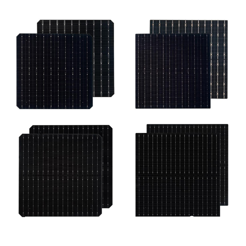
Optimizing stringing and soldering requires immediate attention. We strongly recommend evaluating non-destructive cutting (NDC) laser technology. NDC technology deeply penetrates the silicon structure and snaps it cleanly. This leaves incredibly smooth cell edges. Smooth edges resist cracking far better than rough ones. Additionally, implement low-temperature soldering fluxes or conductive adhesives. These alternatives reduce thermal shock significantly during stringing.
Advanced handling systems are equally vital. You should transition away from rigid pneumatics. Move toward low-stress vacuum automation instead. These newer systems spread suction force evenly across the cell surface. Tension control is especially critical for rectangular formats. Consider the specific handling parameters required for a G12R Solar Cell. You must maintain perfect tension balance along its longer edges. Uneven lifting snaps a rectangular cell instantly.
Finally, update your environmental and conveyor calibrations. Replace outdated rigid conveyor materials entirely. Use flexible, impact-absorbing composites instead. These modern materials cushion the cell during high-speed transit. Strict environmental temperature controls inside the facility also matter. Buffer storage areas often experience harsh temperature drafts. Stabilize these zones to prevent thermal shocking while cells sit in temporary queues.
Table: Production Line Stress Mitigation Strategies
Stress Source | Traditional Method | Recommended Upgrade |
|---|---|---|
Cell Cutting | Standard ablative laser scribing | Non-destructive cutting (NDC) lasers |
Robotic Handling | High-pressure centralized vacuum grippers | Low-stress distributed suction arrays |
Conveyor Transit | Rigid metal or hard plastic belts | Flexible, impact-absorbing composites |
Cell Stringing | High-temperature infrared soldering | Low-temperature conductive adhesives |
Why do standard visual inspections fail? Automated Optical Inspection (AOI) uses standard visual-spectrum cameras. They only see surface-level defects. They easily spot broken busbars or surface stains. However, they entirely miss internal solar cell microcracks hidden beneath metallization grids. You absolutely need Electroluminescence (EL) imaging. EL passes a reverse current through the cell. This forces the silicon to emit near-infrared light. Cracks appear instantly as stark dark lines.
When evaluating EL equipment, you must balance accuracy against speed. Can the EL machine actually keep up? A multi-gigawatt line processes thousands of cells hourly. The inspection unit cannot cause production bottlenecks. Fast imaging sensors are non-negotiable for modern facilities.
Software integration represents another critical evaluation dimension. Human operators cannot review EL images fast enough. They also suffer from severe eye fatigue. You must evaluate AI-driven defect recognition software. AI analyzes EL images in milliseconds. It eliminates subjective human error entirely. The algorithm consistently flags microscopic faults.
Placement strategy determines your ultimate return on investment. Some managers place EL testers only post-lamination for final QA. This is a costly mistake. You should place EL testers pre-lamination instead. This early placement allows you to salvage unlaminated cells. You stop bad cells before you waste expensive glass, EVA encapsulant, and backsheets.
Upgrading your line introduces unavoidable challenges. Production downtime is the most immediate risk. You must halt active lines to retrofit stringers or install new EL stations. Careful scheduling minimizes this disruption. Managers should align equipment upgrades during planned seasonal maintenance windows.
You will also face the false reject dilemma. AI software sometimes acts too sensitive. Overly sensitive AI flags harmless grain boundaries as severe cracks. This causes false positives. Consequently, you waste perfectly viable cells. Calibration phases require intense focus. Your engineers must train the AI model on thousands of varied images. This teaches the system the difference between fatal flaws and benign surface marks.
Operator adoption dictates long-term success. New equipment often requires manual maintenance. You must retrain your floor staff on manual handling protocols. Even highly advanced automated lines need human intervention during equipment jams. Poor manual handling during these specific interventions causes massive human-induced fractures. Staff must understand fragility limits.
We highly recommend a phased rollout strategy. Do not upgrade the entire facility simultaneously. Pilot the upgrades on a single high-stress line first. Choose your newest high-capacity line for this exact test. Master the new thermal profiles and robotic tensions there. Once stable, deploy the proven parameters facility-wide.
Choosing the right partners prevents future manufacturing headaches. Use a strict vendor evaluation matrix to filter your options.
First, demand a proven track record. The vendor must have explicit experience handling ultra-thin wafer architectures. Second, demand transparency regarding AI defect-detection accuracy rates. Ask for real-world case studies showing their false-positive ratios. Third, evaluate their post-installation support rigorously. Local parts availability is crucial. Waiting weeks for a simple replacement vacuum gripper paralyzes your output.
Here are actionable next steps for your engineering team:
Conduct a full-line thermal and mechanical audit immediately.
Use dummy wafers embedded with specialized stress sensors to map your conveyors.
Identify exactly where the highest pressure spikes occur on the belt.
Request pilot testing of your specific cell formats on vendor equipment.
Send sample batches to the vendor to verify their EL detection accuracy firsthand.
Preventing solar cell microcracks is never a single-step fix. It demands a holistic integration strategy. You must combine low-stress physical handling with high-fidelity EL inspection. Modern gigawatt lines leave no margin for error. As wafer sizes increase and thicknesses decrease, traditional manufacturing tolerances become obsolete entirely.
Your final takeaway is straightforward. Upfront investment in process optimization is mandatory. Modernizing your robotics, upgrading your soldering techniques, and deploying AI software cost money initially. However, these investments prevent massive back-end profitability leaks. They dramatically reduce scrap rates and eliminate costly warranty disputes. Ultimately, proactively managing production stress secures long-term module reliability and heavily protects your market reputation.
A: While true zero remains the ultimate goal, acceptable thresholds rely on strict industry severity scoring. Non-critical microcracks typically cover less than 5% of the cell area and do not intersect busbars. Critical cracks extend across metallization lines, threatening immediate power loss. Facilities should aim to keep critical defect rates well below 0.5% pre-lamination.
A: Yes. TOPCon cells generally utilize thinner wafers to maximize cost-efficiency. They also require vastly different, higher-temperature metallization and thermal processing steps. These unique material realities make TOPCon architectures notably more sensitive to process-induced mechanical and thermal stress than standard PERC cells. Careful handling calibration is absolutely essential.
A: No single test offers absolute perfection. EL testing accurately identifies existing fractures before shipping. However, new solar cell microcracks can still propagate later. Rough handling during transportation or improper torque applied during field installation often causes delayed cracking. EL secures the factory floor, but careful downstream handling remains necessary.



